
Depth Map Generation on FPGA
About
Most of the image processing projects in academia has been done on higher-end FPGA’s with a considerable amount of resources. The main objective of this project is to implement a reliable embedded system on a lower end FPGA with limited resources. This project is based on Disparity calculation based on SAD (Sum of Absolute Difference) algorithm and creating a depth map.
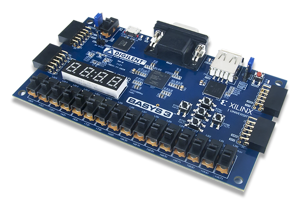
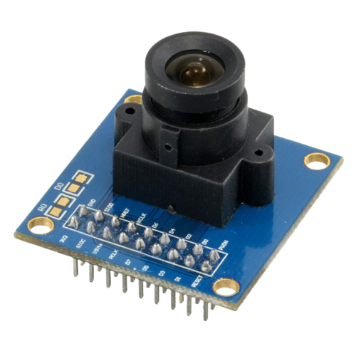
Hardware used for this project
- Basys 3 FPGA board
- 2x OV7670 image sensor modules
This project has 3 major sections
- Functional verification of disparity generator based on Verilog
- Stereo camera implementation using OV7670 sensors based on VHDL
- Real time disparity generation on Basys3 FPGA
Functional verification
Hardware description languages(HDL) are not meant to be for rapid prototyping. Therefore, in this case, I have used python as the prototyping tool. The SAD algorithm was implemented on python from scratch without using any external library. I refrained from using 2D image arrays to store data because then the HDL implementation is straight forward.
SAD/SSD theory
Sum of Absolute difference and Sum of Squared Difference Disparity calculation theory is based on a simple geometric concept. Where they use the stereo vision to calculate the distance to the objects. For the implementation, two cameras should be on the same plane and they should not have any vertical offsets in their alignments.
\[D(x,y,d) = |I_l(x,y)-I_r(x-d,y)|^2\]Python implementation
The python implementation can be found here
Test images used For the functional verification, I have used the most famous stereo image pair “Tsukuba” stereo pair


Left image and Right Tsukuba images
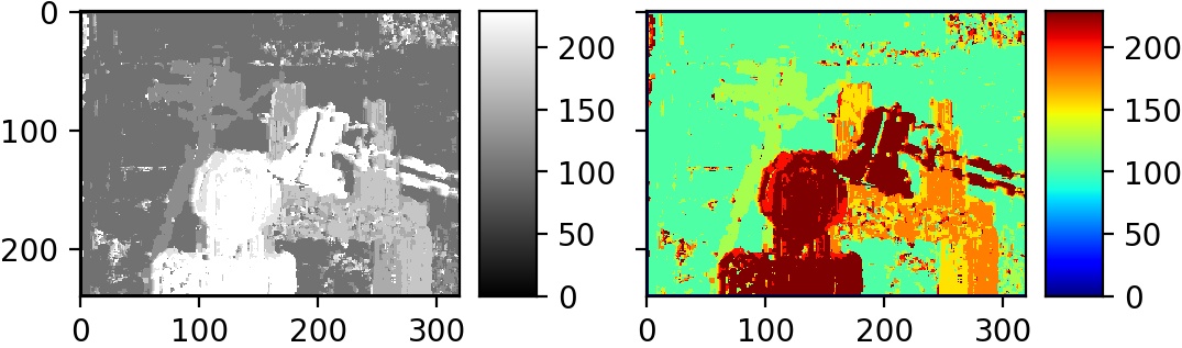
Python results
For this generation, it took more than 4 seconds using an average laptop computer without any accelerating techniques. Based on the Python implementation Abstract flow chart is generated as follows.

Disparity generation Flow chart
Then this algorithm is directly ported to Verilog. The implementation was done using ISE design suite by Xilinx. The image files were converted to hex and imported to the simulation and the output is directly saved as a Bitmap image.

Timing diagrams at 50MHz
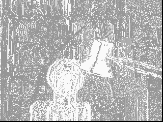
Simulation Output
*** these modules are only for simulation purposes, Do not synthesize the code.
Stereo Camera implementation
The cameras that were used for this project is very inexpensive OV7670 modules. They are commonly available and the output can be configured to 8bit parallel. These cameras are using I2C interface to communicate with the master. We can configure the camera output by changing the internal registers of the cameras.
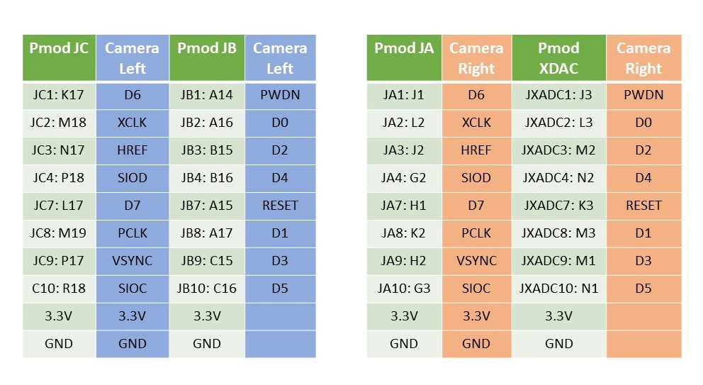
Pmod connections with Cameras
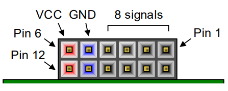
Pmod connector pinouts
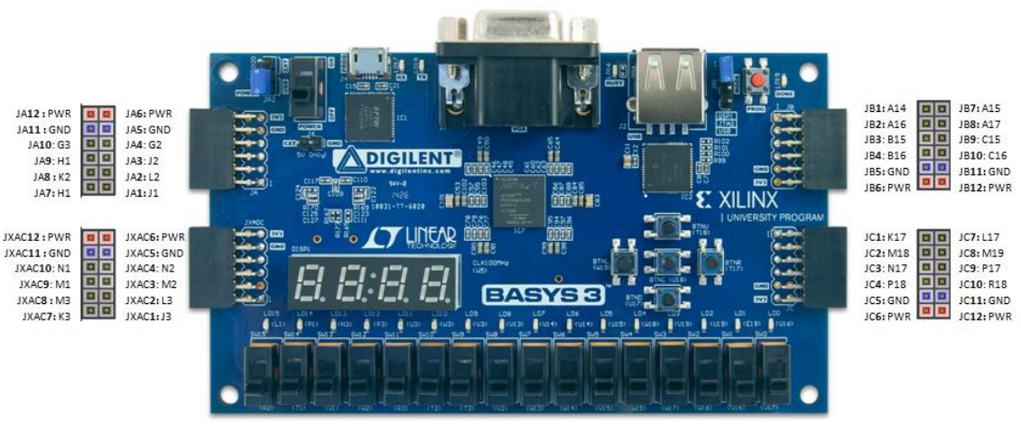
Basys3 Pmod pinout diagram
This repo contains VHDL implementation for image read from two cameras and displaying the average of two images from the VGA output.
OV7670 dual camera mount was designed using a cad tool and 3D printed to mount the cameras. STL files for camera mount can be found from here.
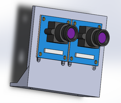
CAD Stereo camera mount

Hardware connected together
Camera configuration
OV7670 camera module comes with I2C interface to configure it’s internal registers. The problem here is we are using two cameras with the same type. By taking the advantage of paralel hardware implementation on FPGA two seperate I2C buses were used for the dual camera intergration. Fortunatly prioir work related to OV7670 Camera intergration to Zedboard FPGA has been done by the Engineer Mike Field at here. This I2C driver was direcly ported to the Basys3 FPGA. Camera register configuration was done inorder to get required output from the Camera.
Real-time depth map generation on FPGA
When converting the functional verification module into synthesizable code due to limited functionalities in Verilog, VHDL was selected as the developing language.
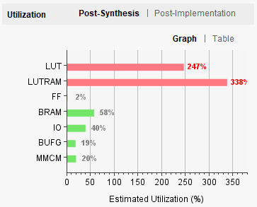
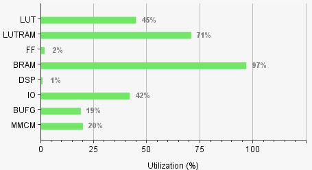
Resource Utilization
Basys 3 is a entry level FPGA board. Hence it is not designed for image processing tasks. The Challange here was to run complex image processing algorithm on limited resources. Basys 3 Trainer FPGA board consists of following resources.
| Resource | Available |
|---|---|
| LUT | 20800 |
| LUTRAM | 9600 |
| FF | 41600 |
| BRAM | 50 |
| DSP | 90 |
| IO | 106 |
| BUFG | 32 |
| MMCM | 5 |
The main bottle necks were the Block memory and the LUTRAM. Basys 3 has 1,800Kbits of memory in 50 cells as 36,000bits in each cell. We are getting the camera output in YCbCr format. Here Y is the gray scale image of individual pixel size 4bits.
Memory requirement calculation
For left image : 320x240x4 bits
For right image : 320x240x4 bits
For Average image : 320x240x4 bits
For Disparity image : 320x240x8 bits
Total memory required : 1,536,000 bits/1,800 000 bits
We cant process them images while it is in the BRAM because BRAM is FIFO (First In First Out) memory device. Therefor the Image sholud be loaded in a cache so that data can be accessed parallely. The cache can be created using the LUTRAM. The problem we have is the LUTRAM is insufficient to store two 320x240 images. Even the 160x120 size images cannot be stored to support SAD algorithm to compare.
LUT bottleneck for 160x120 resolution
Therefore a blockwise disparity calculation was used in order to utilize the full 320x240 resolution with available resources. The caching is done in block wise and then the caculated dispairty values are saved to the disparity_buffer circuit.
- Although there are 9600 LUTRAMS are available we cannot ulilize 100% of that due to routing issues.

Routing failure
Blockwise disparity calculation Utilization at 320x240 resolution
VGA Output
The system outputs the generated disparity map using the VGA output of the FPGA. Following are recorded output from the monitor using a camera.
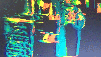
Demo -1

Demo -2
In both the demonstrations you may observe that camera exposure changes with the environement changes. Improvements are needed to fix this. It will reduce the noise in the output. Auto Exposure Correction (AEC) has been disabled from the cameras by editing the internal register modules. After disableing AEC, the result was much more clear and the noise was removed from the background.
Image Rectification and Camera Caliberation
The offsets of the two cameras are fixed using a image rectification module. Although the Automatic Exposure Caliberation is turned of one of the Cameras output is very darker while the other one is too bright. This should be corrected for the Disparity aldorithm to work correctly.
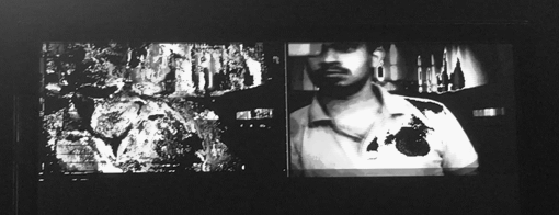
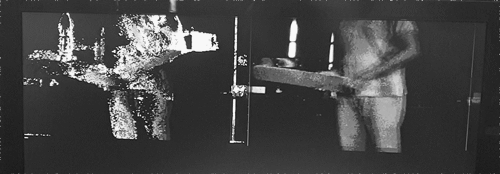
Demo -3 ( Left : Disparity output | Right : average image of two cameras )
If we observe closely left camera brightness is too lower than the right hand side camera.
After caliberation of exposure in cameras individually and improving the Image rectification module final output was in a good condition. There are noice and miss calculated points due to the inability of the cameras to identify the features correctly. But the output is smooth and clear.
Demo -4 ( Left : Disparity output | Right : average image of two cameras )
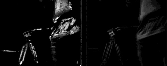
Optimized system demo ( Left : Disparity output | Right : average image of two cameras )
Cite this work
Jayasena, A., 2021. Register Transfer Level Disparity generator with Stereo Vision. Journal of Open Research Software, 9(1), p.18. DOI: http://doi.org/10.5334/jors.339
Citation (bibtex) [Switch view]@article{Jayasena_2021,
	doi = {10.5334/jors.339},
	url = {https://doi.org/10.5334/jors.339},
	year = 2021,
	publisher = {Ubiquity Press, Ltd.},
	volume = {9},
	author = {Aruna Jayasena},
	title = {Register Transfer Level Disparity generator with Stereo Vision},
	journal = {Journal of Open Research Software}
}